| CPC G02F 1/136286 (2013.01) [G02F 1/1368 (2013.01)] | 18 Claims |

|
1. A display panel, comprising an array substrate and an opposite substrate which are cell-assembled, wherein,
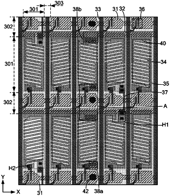
the array substrate comprises a first substrate, and a scanning line, a data line, a first barrier wall and a second barrier wall which are formed at a side of the first substrate close to the opposite substrate; the data line extends in a first direction, the scanning line extends in a second direction, and the first direction intersects with the second direction; the first barrier wall and the second barrier wall are located at opposite sides of the scanning line in the first direction, respectively, and each of the first barrier wall and the second barrier wall comprises a first barrier layer which is arranged in the same layer as the scanning line and spaced apart from the scanning line, and a second barrier layer which arranged in the same layer as the data line and spaced apart from the data line; an orthographic projection of the second barrier layer on the first substrate overlaps with an orthographic projection of the first barrier layer on the first substrate; a distance between the first barrier layer and the scanning line in the first direction is a first distance, and a distance between the second barrier layer and the scanning line in the first direction is a second distance, the second distance is larger than the first distance,
the opposite substrate comprises a second substrate and a spacer located at a side of the second substrate close to the array substrate, a surface of the spacer close to the first substrate is a top surface, and an orthographic projection of the top surface of the spacer is located within an orthographic projection of the scanning line on the first substrate, and located between the orthographic projection of the first barrier wall on the first substrate and the orthographic projection of the second barrier wall on the first substrate; and a size of the top surface of the spacer in the first direction is larger than the first distance;
the array substrate further comprises a plurality of sub-pixel units, each of the plurality of sub-pixel units comprises a pixel electrode, the pixel electrode comprises a conductive connection portion, a first electrode portion comprising a first connection bar extending in the first direction and a plurality of first electrode strips arranged at intervals in the first direction; a second electrode portion spaced apart from the first electrode portion in the first direction, wherein the second electrode portion comprises a second connection bar extending in the first direction and a plurality of second electrode strips spaced apart in the first direction,
the conductive connection portion comprises a first conductive connection bar and a second conductive connection bar which are arranged at intervals in the second direction and both extend in the first direction, and at least two third conductive connection bars located between the first conductive connection bar and the second conductive connection bar and arranged at intervals in the first direction, and two ends of each of the third conductive connection bars are connected with the first conductive connection bar and the second conductive connection bar, respectively,
wherein the first conductive connection bar is connected with the first connection bar, and the second conductive connection bar is connected with the second connection bar.
|