| CPC G02F 1/133606 (2013.01) [G02B 6/0016 (2013.01); G02B 6/0021 (2013.01); G02B 6/003 (2013.01); G02B 6/0036 (2013.01); G02B 6/0055 (2013.01); G02B 6/0073 (2013.01); G02B 6/0083 (2013.01); G02F 1/133605 (2013.01); G02F 1/133608 (2013.01); G02F 1/133611 (2013.01); H01L 25/0753 (2013.01); G02B 6/0043 (2013.01); G02B 6/0068 (2013.01); G02F 1/133603 (2013.01); G02F 1/133607 (2021.01); G02F 1/133614 (2021.01); H01L 25/0756 (2013.01); H01L 33/46 (2013.01); H01L 33/502 (2013.01); H01L 33/507 (2013.01); H01L 33/54 (2013.01); H01L 33/60 (2013.01); H01L 33/62 (2013.01); H01L 2933/0091 (2013.01)] | 18 Claims |

|
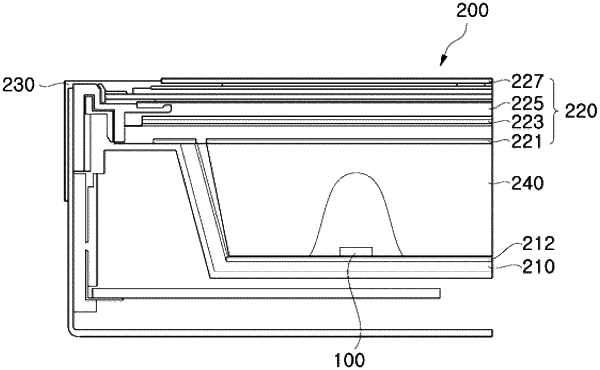
1. A backlight module comprising:
a frame;
a substrate disposed on the frame;
a light emitting diode disposed on the substrate and including an upper region, a lower region facing the substrate, and a side region disposed between the upper region and the lower region;
an optical part disposed over the upper region of the light emitting diode and including at least one of a wavelength conversion sheet or an optical sheet;
a light guider disposed between the frame and the optical part to cover the upper region of the light emitting diode;
a reflector disposed between the frame and the light guider, the reflector being configured to reflect at least a part of a light emitted from the light emitting diode to direct at least the part of the light to the light guider; and
a first-type electrode and a second type electrode,
wherein the light emitting diode includes a first-type semiconductor layer electrically connected to the first-type electrode and a second-type semiconductor layer electrically connected to the second-type electrode,
wherein the light guider includes a light exit that has a grooved region, and
wherein the grooved region of the light exit covers an upper surface of the light emitting diode.
|