| CPC G02F 1/133512 (2013.01) [G02F 1/133528 (2013.01); G02F 1/13452 (2013.01); G02F 1/13458 (2013.01); H10K 50/865 (2023.02); G02F 1/133531 (2021.01)] | 11 Claims |

|
1. A display device comprising:
a display panel including:
an active area displaying an image; and
a peripheral area surrounding the active area;
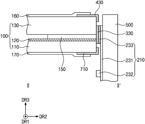
a first light blocking layer disposed on a portion of the peripheral area adjacent to a first side surface of the display panel;
a second light blocking layer disposed under a portion of the peripheral area adjacent to a second side surface of the display panel, the second side surface connecting the first side surface;
an upper polarizing film disposed on the display panel, covering a portion of the first light blocking layer and having a first absorption axis; and
a lower polarizing film disposed under the display panel and having a second absorption axis intersecting the first absorption axis of the upper polarizing film, wherein
the first absorption axis of the upper polarizing film is parallel to a first direction,
the first side surface of the display panel is spaced apart from the upper polarizing film in the first direction in a plan view, and
a portion of the second light blocking layer is covered by the lower polarizing film.
|