| CPC G02F 1/0105 (2013.01) [G02F 1/01791 (2021.01); G02F 1/13394 (2013.01); G02F 1/133512 (2013.01); G02F 1/133614 (2021.01); G02F 2201/50 (2013.01); H10K 59/35 (2023.02); H10K 59/38 (2023.02)] | 20 Claims |
|
1. A display device comprising:
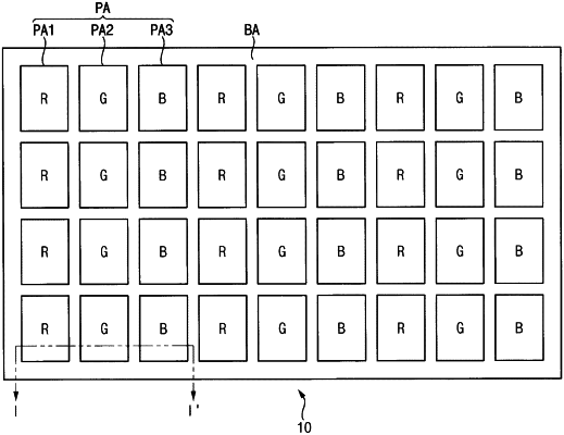
a lower substrate including first and second pixel areas and a light shielding area surrounding the first and second pixel areas;
a light emitting structure disposed on the lower substrate;
an upper substrate disposed on the light emitting structure;
a first color conversion layer disposed in the first pixel area on a bottom surface of the upper substrate;
a second color conversion layer disposed in the second pixel area on the bottom surface of the upper substrate;
first to third light shielding patterns disposed in the light shielding area on the bottom surface of the upper substrate;
a groove defined on a bottom surface of at least one selected from the first to third light shielding patterns; and
a spacer disposed in the groove, wherein a height of the spacer is greater than a depth of the groove.
|