| CPC G02B 6/4206 (2013.01) [G02B 6/122 (2013.01); G02B 6/132 (2013.01); G02B 6/42 (2013.01); G02B 6/4212 (2013.01); G02B 6/4225 (2013.01); G02B 6/428 (2013.01); H01L 25/167 (2013.01)] | 18 Claims |
|
1. A semiconductor package, comprising:
a first interconnect layer comprising a first dielectric material;
a cavity defined by a removal of a first portion of the first dielectric material;
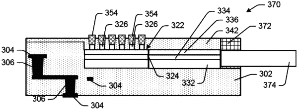
an embedded optical die deposited in the cavity;
a waveguide deposited adjacent to the embedded optical die in the cavity;
a core portion sandwiched between cladding portions, wherein the core portion is aligned with an optical output of the embedded optical die, and the cladding portions are formed by depositing optical epoxy adjacent to the embedded optical die within the cavity;
a second cavity that is defined by removing a second portion of the second dielectric material;
an optical fiber included in the second cavity, wherein direct coupling to the embedded optical die is avoided by not surface mounting the embedded optical die; and
a second dielectric material deposited in a manner to fill open portions of the cavity in which the embedded optical die and waveguide are deposited providing a substantially planarized top surface of the first interconnect layer.
|