| CPC G02B 26/105 (2013.01) [B81C 1/00317 (2013.01); B81C 1/00523 (2013.01); G02B 26/0833 (2013.01); B81B 2201/042 (2013.01); B81C 2203/0109 (2013.01); B81C 2203/019 (2013.01)] | 20 Claims |

|
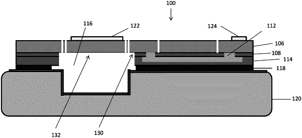
1. A method of making a micro-electro mechanical system (MEMS) device, comprising:
forming a MEMS mirror stack on a handle layer;
applying a first bonding layer to the MEMS mirror stack;
disposing a substrate on the first bonding layer to mechanically anchor the MEMS mirror stack to the substrate and seal against ingress of environmental contaminants;
removing the handle layer;
applying a second bonding layer to the MEMS mirror stack; and
disposing a cap layer on the second bonding layer to mechanically anchor the cap layer to the MEMS mirror stack and seal against ingress of environmental contaminants;
wherein forming the MEMS mirror stack comprises:
disposing a silicon layer on the handle layer;
disposing a first insulating layer on the silicon layer;
etching portions of the first insulating layer;
depositing a first conductive layer on the first insulating layer and into the etched portions thereof, the first conductive layer deposited so as to have a width greater than a width of the substrate in at least one direction;
depositing a second insulating layer on the first conductive layer;
removing at least one portion of the second insulating layer to expose at least one portion of the first conductive layer exposed due to the first conductive layer having a width greater than the width of the substrate in the at least one direction; and
forming a conductive pad on the at least one exposed portion of the first conductive layer and extending away from the MEMS mirror stack opposite the cap layer.
|