| CPC G01N 27/221 (2013.01) [G01R 31/24 (2013.01); G01R 31/2648 (2013.01); H01L 22/14 (2013.01); H01L 27/14 (2013.01)] | 20 Claims |
|
1. A method of characterizing a wide-bandgap semiconductor material, comprising:
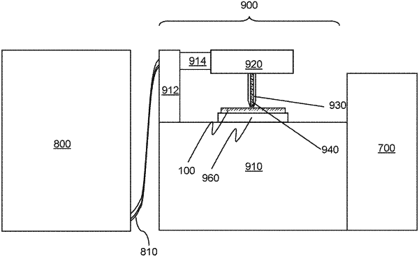
providing a substrate which contains a capacitor structure including a layer stack of a first electrode as embodied as a conductive material layer, a node dielectric as embodied as a dielectric material layer, and a second electrode as embodied as a wide-bandgap semiconductor material layer;
disposing a tip of a mercury probe on the top surface of the wide-bandgap semiconductor material layer;
generating a set of multiple alternating-current (AC) capacitance curves of the layer stack that represents a change in AC capacitance as a function of a change in a direct-current (DC) bias voltage across the conductive material layer and the wide bandgap semiconductor material layer by applying a combination of the DC bias voltage and a sinusoidal alternating-current (AC) perturbation voltage across the layer stack, wherein the multiple AC capacitance curves are generated using different frequencies for the sinusoidal AC perturbation voltage; and
determining a structural parameter of the wide-bandgap semiconductor material layer which is selected from porosity, crystallinity, stoichiometry, and thickness by correlating observed features within the set of multiple AC capacitance curves with the structural parameter using a database containing information on previously-established correlation between features among sets of multiple AC capacitance curves and structural parameters of a reference compound semiconductor material layer having a same base composition as the wide-bandgap semiconductor material layer in the layer stack.
|