| CPC G01L 1/247 (2013.01) [G01L 1/241 (2013.01); H05K 1/0274 (2013.01); H05K 1/141 (2013.01); H05K 1/181 (2013.01); H05K 2201/0367 (2013.01); H05K 2201/10151 (2013.01)] | 17 Claims |
|
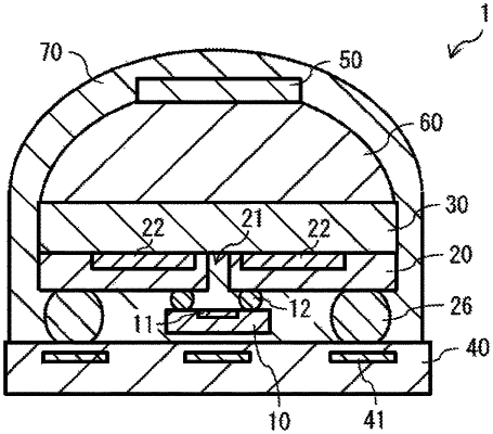
1. An optical sensor comprising:
a light emitting substrate including a light emitting device;
a circuit board provided at a position opposing the light emitting device, the circuit board including a light transmitting section and one or multiple light receiving devices, the light transmitting section transmitting light of the light emitting device, the one or multiple light receiving devices receiving light reflected by a reflective layer of the light of the light emitting device exiting through the light transmitting section,
wherein the one or multiple light receiving devices are formed on a first major surface of the circuit board, and
the light emitting substrate is disposed at a position opposing a second major surface, of the circuit board, on an opposite side to the first major surface, and is stacked on the circuit board with a first bump interposed therebetween, and
wherein the circuit board further includes a control circuit and a processing circuit, the control circuit controlling light emission of the light emitting device, the processing circuit processing a light reception signal obtained by the one or multiple light receiving devices; and
a wiring substrate including a wiring line adapted to electrically coupling an external circuit and each of the control circuit and the processing circuit, the wiring substrate being disposed at a position opposing the circuit board with the light emitting substrate interposed therebetween and being stacked on the circuit board with a second bump interposed therebetween.
|