| CPC G01K 7/015 (2013.01) [H01L 21/02532 (2013.01); H01L 21/02603 (2013.01); H01L 21/26513 (2013.01); H01L 21/82285 (2013.01); H01L 27/0826 (2013.01); H01L 29/0673 (2013.01); H01L 29/165 (2013.01); H01L 29/66242 (2013.01); H01L 29/7371 (2013.01)] | 20 Claims |
|
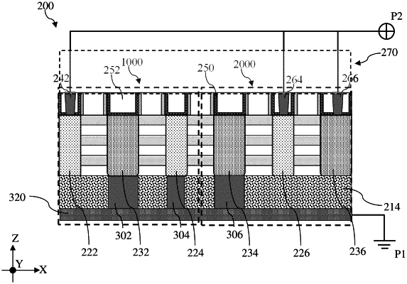
1. A semiconductor device, comprising:
a dielectric layer; and
a fin-shaped structure disposed over the dielectric layer, the fin-shaped structure comprising:
a first p-type doped region, a second p-type doped region, and a third p-type doped region, and
a first n-type doped region, a second n-type doped region, and a third n-type doped region interleaving the first p-type doped region, the second p-type doped region, and the third p-type doped region,
wherein the first p-type doped region, the third p-type doped region and the third n-type doped region are electrically coupled together to a first potential,
wherein the second p-type doped region, the first n-type doped region and the second n-type doped region are electrically coupled together to a second potential different from the first potential.
|