US 12,078,308 B2
Lighting device
Kwang Ho Park, Seoul (KR); Chul Hong Kim, Seoul (KR); Hyun Duck Yang, Seoul (KR); Moo Ryong Park, Seoul (KR); and Jun Chul Hyun, Seoul (KR)
Assigned to LG INNOTEK CO., LTD., Seoul (KR)
Filed by LG Innotek Co., Ltd., Seoul (KR)
Filed on Jul. 11, 2023, as Appl. No. 18/350,450.
Application 18/350,450 is a continuation of application No. 17/647,302, filed on Jan. 6, 2022, granted, now 11,739,899.
Application 17/647,302 is a continuation of application No. 16/819,656, filed on Mar. 16, 2020, granted, now 11,248,764, issued on Feb. 15, 2022.
Application 16/819,656 is a continuation of application No. 15/900,358, filed on Feb. 20, 2018, granted, now 10,627,064, issued on Apr. 21, 2020.
Application 15/900,358 is a continuation of application No. 15/495,433, filed on Apr. 24, 2017, granted, now 9,933,126, issued on Apr. 3, 2018.
Application 15/495,433 is a continuation of application No. 14/742,207, filed on Jun. 17, 2015, granted, now 9,664,844, issued on May 30, 2017.
Application 14/742,207 is a continuation of application No. 13/920,844, filed on Jun. 18, 2013, granted, now 9,086,209, issued on Jul. 21, 2015.
Claims priority of application No. 10-2012-0065259 (KR), filed on Jun. 18, 2012; application No. 10-2012-0065260 (KR), filed on Jun. 18, 2012; and application No. 10-2012-0065264 (KR), filed on Jun. 18, 2012.
Prior Publication US 2023/0349526 A1, Nov. 2, 2023
This patent is subject to a terminal disclaimer.
Int. Cl. F21S 41/20 (2018.01); B60Q 1/00 (2006.01); F21S 41/19 (2018.01); F21S 41/30 (2018.01); F21S 41/32 (2018.01); F21S 41/663 (2018.01); F21S 43/14 (2018.01); F21S 43/15 (2018.01); F21S 43/19 (2018.01); F21S 43/20 (2018.01); F21S 43/30 (2018.01); F21V 3/02 (2006.01); F21V 3/04 (2018.01); F21V 8/00 (2006.01); F21V 13/02 (2006.01); F21V 13/08 (2006.01); F21V 15/01 (2006.01); F21V 29/503 (2015.01); F21V 29/70 (2015.01); H01L 25/075 (2006.01); H01L 33/48 (2010.01); H01L 33/56 (2010.01); H01L 33/58 (2010.01); H01L 33/60 (2010.01); H01L 33/62 (2010.01); B60Q 1/04 (2006.01); B60Q 1/26 (2006.01); B60Q 1/30 (2006.01); F21V 31/04 (2006.01); F21Y 105/10 (2016.01); F21Y 115/10 (2016.01)
CPC F21S 41/20 (2018.01) [B60Q 1/0011 (2013.01); F21S 41/192 (2018.01); F21S 41/30 (2018.01); F21S 41/32 (2018.01); F21S 41/663 (2018.01); F21S 43/14 (2018.01); F21S 43/15 (2018.01); F21S 43/195 (2018.01); F21S 43/20 (2018.01); F21S 43/30 (2018.01); F21V 3/02 (2013.01); F21V 3/04 (2013.01); F21V 13/02 (2013.01); F21V 13/08 (2013.01); F21V 15/012 (2013.01); F21V 29/503 (2015.01); F21V 29/70 (2015.01); G02B 6/0031 (2013.01); G02B 6/0051 (2013.01); G02B 6/0055 (2013.01); G02B 6/0083 (2013.01); G02B 6/0085 (2013.01); G02B 6/0088 (2013.01); G02B 6/0095 (2013.01); H01L 25/0753 (2013.01); H01L 33/48 (2013.01); H01L 33/56 (2013.01); H01L 33/58 (2013.01); H01L 33/60 (2013.01); H01L 33/62 (2013.01); B60Q 1/04 (2013.01); B60Q 1/2696 (2013.01); B60Q 1/30 (2013.01); F21V 31/04 (2013.01); F21Y 2105/10 (2016.08); F21Y 2115/10 (2016.08); H01L 2224/48091 (2013.01); H01L 2224/48247 (2013.01)] 17 Claims
OG exemplary drawing
 
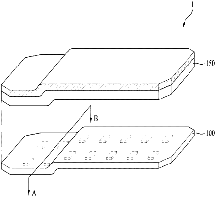
1. A lighting device comprising:
a board;
a plurality of light sources disposed on the board;
a reflection unit disposed on the board;
a resin layer disposed on the board so that the plurality of light sources is embedded therein;
a reflector disposed on a side surface of the resin layer; and
an optical pattern layer disposed on the resin layer,
wherein the optical pattern layer comprises a first optical sheet disposed on the resin layer, a second optical sheet disposed on the first optical sheet, an optical pattern disposed between the first optical sheet and the second optical sheet, an adhesive pattern layer disposed between the first optical sheet and the second optical sheet, and a second spacing part disposed between the first optical sheet and the second optical sheet,
wherein the second spacing part is disposed between the optical pattern and the adhesive pattern layer, and
wherein the second spacing part is disposed between the optical pattern and the first optical sheet.