| CPC C23C 14/042 (2013.01) [B05D 1/32 (2013.01); B05D 5/06 (2013.01); C23C 14/08 (2013.01); Y10T 29/49826 (2015.01)] | 16 Claims |

|
1. A method of manufacturing a mask assembly, comprising:
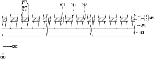
forming a cell mask comprising a plurality of masking patterns and a mesh frame comprising a plurality of conductive patterns disposed to correspond to the plurality of masking patterns; and
disposing the cell mask and the mesh frame on a mask frame, the forming the cell mask and the mesh frame comprising:
forming a polymer layer on a base substrate;
forming a conductive layer directly on the polymer layer;
forming a hard masking layer directly on the conductive layer, the hard masking layer comprising a first polymer material;
etching the hard masking layer and the conductive layer and forming a mask pattern layer comprising etch patterns; and
etching the polymer layer using the mask pattern layer and forming the cell mask and the mesh frame.
|