US 12,077,699 B2
Dopant for organic optoelectronic device, organic optoelectronic device, and display device
Sangshin Lee, Suwon-si (KR); Mounggon Kim, Suwon-si (KR); Eun Sun Yu, Suwon-si (KR); and Jun Yeob Lee, Suwon-si (KR)
Assigned to SAMSUNG SDI CO., LTD., Yongin-si (KR)
Appl. No. 15/573,977
Filed by SAMSUNG SDI CO., LTD., Yongin-si (KR)
PCT Filed Oct. 26, 2015, PCT No. PCT/KR2015/011321
§ 371(c)(1), (2) Date Nov. 14, 2017,
PCT Pub. No. WO2016/186269, PCT Pub. Date Nov. 24, 2016.
Claims priority of application No. 10-2015-0068121 (KR), filed on May 15, 2015.
Prior Publication US 2018/0291264 A1, Oct. 11, 2018
Int. Cl. C07D 209/62 (2006.01); C07D 265/38 (2006.01); C07D 403/14 (2006.01); C07D 413/14 (2006.01); C09K 11/06 (2006.01); H10K 50/11 (2023.01); H10K 85/60 (2023.01)
CPC C09K 11/06 (2013.01) [C07D 209/62 (2013.01); C07D 265/38 (2013.01); C07D 403/14 (2013.01); C07D 413/14 (2013.01); H10K 85/654 (2023.02); H10K 85/6572 (2023.02); C09K 2211/1007 (2013.01); C09K 2211/1018 (2013.01); H10K 50/11 (2023.02)] 2 Claims
OG exemplary drawing
 
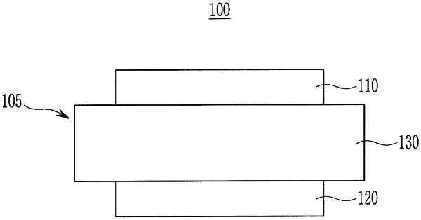
1. An organic optoelectronic device, comprising:
an anode and a cathode facing each other, and a light emitting layer disposed between the anode and the cathode, the light emitting layer including:
a host, and
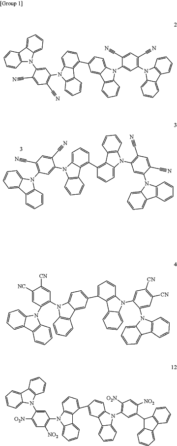
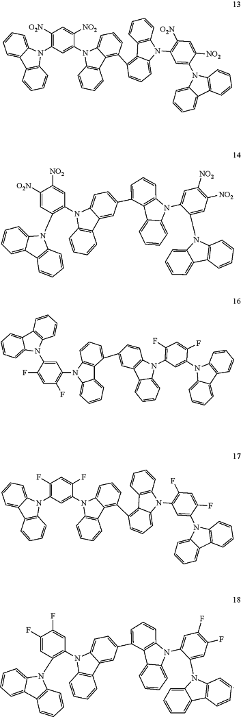
a dopant, the dopant being a compound of Group 1 [Grou 1′] wherein:
the host is selected from the compound having a larger energy bandgap than the dopant,
the dopant is included in an amount of 0.01 wt % to 40 wt % based on a total amount of the host and the dopant, provided that the dopant is included in a smaller amount than the host,

OG Complex Work Unit Chemistry

OG Complex Work Unit Chemistry