| CPC B81C 1/00325 (2013.01) [B81B 3/001 (2013.01); B81C 1/00523 (2013.01); B81B 2203/0315 (2013.01); B81C 2203/0145 (2013.01)] | 12 Claims |

|
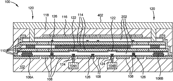
1. A method of manufacturing a MEMS device, comprising:
forming one or more electrical contact stacks comprising a contact surface of ruthenium, at least one of the one or more electrical contact stacks formed over at least one contact electrode;
placing a sacrificial material over the one or more electrical contact stacks;
forming a beam structure over the one or more electrical contact stacks so that the one or the more electrical contacts contact stacks are formed within a cavity that is filled with the sacrificial material;
removing sacrificial material to free the beam structure to move within a cavity, wherein at least one contact portion of the beam structure is capable of contacting the contact surface of the at least one contact electrode;
etching a portion of the contact surface of ruthenium within the cavity using an etchant comprising chlorine; and
sealing the cavity.
|