| CPC B81B 3/0062 (2013.01) [G06F 30/27 (2020.01); B81B 2201/018 (2013.01); B81B 2203/0118 (2013.01); B81B 2203/051 (2013.01); B81B 2203/053 (2013.01); B81B 2203/056 (2013.01); G06F 2111/10 (2020.01)] | 14 Claims |

|
1. An electrical device comprising:
a defect doped material forming at least a portion of an electrical circuit; and
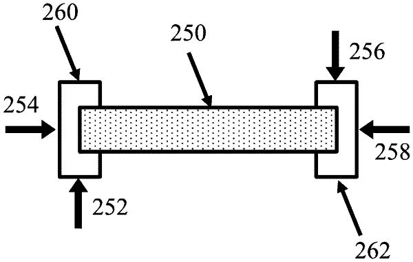
one or more actuators configured to selectively apply a multiaxial strain to at least a first portion of the defect doped material, wherein the defect doped material is a non-conducting material when the defect doped material is in an unstrained state, and wherein at least a second portion of the defect doped material is a semiconducting material or a conducting material when the one or more actuators apply the multiaxial strain to the defect doped material in a strained state,
wherein an activation energy to ionize defects of the defect doped material in the strained state is less than the activation energy to ionize the defects when the defect doped material is in the unstrained state.
|