| CPC A61B 8/4494 (2013.01) [A61B 8/14 (2013.01); A61B 8/145 (2013.01); A61B 8/4483 (2013.01); A61B 8/4488 (2013.01); A61B 8/54 (2013.01); A61N 7/00 (2013.01); A61N 7/02 (2013.01); B06B 1/02 (2013.01); B81C 1/00246 (2013.01); G01S 7/52019 (2013.01); G01S 7/52034 (2013.01); G01S 7/52047 (2013.01); G01S 7/5208 (2013.01); G01S 15/02 (2013.01); G01S 15/8915 (2013.01); G01S 15/8977 (2013.01); H04R 1/00 (2013.01); A61B 8/485 (2013.01)] | 20 Claims |

|
16. A hand-held ultrasound device for placement on a subject, the hand-held ultrasound
device comprising:
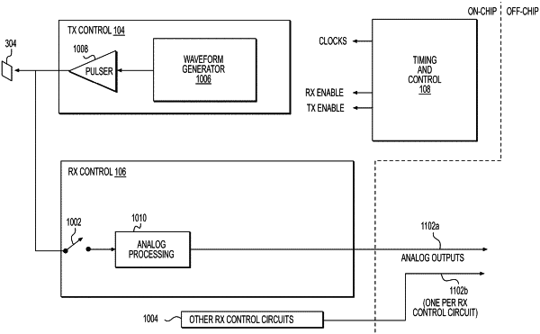
a semiconductor device including:
a plurality of ultrasonic transducer elements;
a plurality of pulsers coupled to the plurality of ultrasonic transducer elements; and
a plurality of waveform generators configured to drive the plurality of pulsers;
receive processing circuitry configured to process ultrasound signals received by the plurality of ultrasonic transducer elements; and
a plurality of independently controllable registers configured to store a plurality of different parameters for the waveform generators; and
a housing to support the semiconductor device, wherein
the plurality of ultrasonic transducer elements comprises a first ultrasonic transducer element and a second ultrasonic transducer element,
the plurality of pulsers comprises:
a first pulser coupled to the first ultrasonic transducer element so that the first ultrasonic transducer element emits an ultrasonic pulse; and
a second pulser coupled to the second ultrasonic transducer element so that the second ultrasonic transducer element emits an ultrasonic pulse,
a first waveform generator of the plurality of waveform generators is coupled to the first pulser to provide a first waveform to the first pulser in response to receipt, by a first transmit control circuit of the semiconductor device, of a transmit enable signal,
a second waveform generator of the plurality of waveform generators is coupled to the second pulser to provide a second waveform to the second pulser in response to receipt, by a second transmit control circuit of the semiconductor device, of the transmit enable signal; and
the semiconductor device further includes:
at least one first delay component that impacts a length of a first delay between when the first transmit control circuit receives the transmit enable signal and when the first waveform is applied to the first pulser; and
at least one second delay component that impacts a length of a second delay between when the second transmit control circuit receives the transmit enable signal and when the second waveform is applied to the second pulser,
wherein the at least one first delay component is configured differently than the at least one second delay component, so that the length of the second delay is different than the length of the first delay.
|