| CPC H10N 52/80 (2023.02) [H10B 61/22 (2023.02); H10N 50/85 (2023.02); H10N 52/00 (2023.02); H10N 52/01 (2023.02)] | 20 Claims |

|
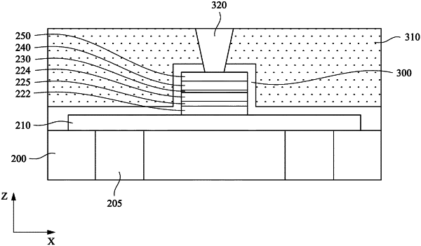
1. A method of manufacturing a spin-orbit-torque (SOT) magnetic device, the method comprising:
forming bottom electrodes in a first interlayer dielectric (ILD) layer;
forming a bottom metal layer directly on the bottom electrodes and fully covering an upper surface of the ILD layer;
forming a first layer for a first magnetic layer directly on the bottom metal layer,
wherein the first layer for the first magnetic layer includes a lower magnetic layer, a middle layer made of non-magnetic layer, a first interfacial layer disposed between the lower magnetic layer and the middle layer, an upper magnetic layer and a second interfacial layer disposed between the middle layer and the upper magnetic layer, and
at least one of the first and second interfacial layers is made of FeB;
forming a second layer for a spacer layer over the first layer;
forming a third layer for a second magnetic layer over the second layer;
forming a fourth layer for an upper electrode over the third layer;
patterning the fourth, third, second and first layers to form a SOT cell structure disposed on the bottom metal layer connecting the bottom electrodes such that the first magnetic layer is in direct contact with the bottom metal layer;
forming a cover layer to cover a top and sides of the SOT cell structure and a surface of the bottom metal layer; and
forming a second ILD layer over the cover layer,
wherein the bottom metal layer and the first ILD layer are separated from the second ILD layer by the cover layer.
|