| CPC H10N 50/01 (2023.02) [G01R 33/093 (2013.01); G11C 11/161 (2013.01); G11C 11/5607 (2013.01); H10B 61/00 (2023.02); H10N 50/10 (2023.02); H10N 50/80 (2023.02); H10N 50/85 (2023.02); G01R 33/0052 (2013.01); G01R 33/098 (2013.01)] | 16 Claims |

|
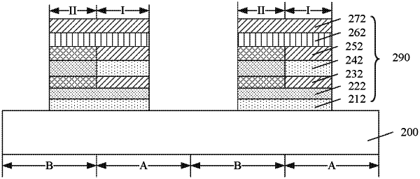
1. A semiconductor structure, comprising:
a substrate; and
magnetic tunnel junctions on the substrate, wherein:
each magnetic tunnel junction of the magnetic tunnel junctions includes a first region and a second region adjacent to the first region, the first region and the second region being coplanar with each other;
each magnetic tunnel junction includes a multilayered material including material layers stacked along a normal direction of the substrate, the material layered being stacked at both the first region and the second region, and the multilayered material including a first electromagnetic layer, an insulating layer over the first electromagnetic layer, and a second electromagnetic layer over the insulating layer;
the material layers of each magnetic tunnel junction include at least one material layer that is different in the first region and the second region, the at least one material layer at the second region being made of a material with doping ions, and the at least one material layer at the first region being made of the material without the doping ions;
the first electromagnetic layer in the first region is made of a material including cobalt iron boron without the doping ions, and the first electromagnetic layer in the second region is made of a material including cobalt iron boron doped with first modifying ions, the first modifying ions including titanium ions, tantalum ions, or a combination thereof;
the second electromagnetic layer in the first region is made of a material including cobalt iron boron without the doping ions, and the second electromagnetic layer in the second region is made of a material including cobalt iron boron doped with second modifying ions, the second modifying ions including titanium ions, tantalum ions, or a combination thereof; and
the multilayered material further includes:
a seed layer covering a bottom surface of the first electromagnetic layer in both the first region and the second region, the seed layer being made of a material including cobalt iron boron;
an optimized layer covering a top surface of the second electromagnetic layer in both the first region and the second region, the optimized layer being made of a material including cobalt iron boron;
a lower electrode layer covering a bottom surface of the seed layer and on a top surface of the substrate; and
an upper electrode layer covering a top surface of the optimized layer.
|