| CPC H10K 59/88 (2023.02) [H10K 50/824 (2023.02); H10K 50/844 (2023.02); H10K 59/122 (2023.02); H10K 59/1315 (2023.02); H10K 59/352 (2023.02); H10K 59/353 (2023.02); H10K 71/00 (2023.02); H10K 59/1201 (2023.02)] | 17 Claims |

|
1. A display device, comprising:
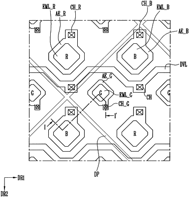
a substrate including a display region and a non-display region, the display region including a plurality of first pixels of a first type, a plurality of second pixels of a second type, and a plurality of third pixels of a third type, each of the first to third pixels having:
an emission region from which light is to be emitted;
a light emitting element in the emission region;
one or more pixel electrodes; and
a pixel circuit area to drive the light emitting element;
a dummy pattern extending through a non-emission region of the substrate located in the display region between adjacent pixels among any two or more of the first pixels, the second pixels and the third pixels, and disposed directly on a pixel defining layer that includes openings exposing a portion of the respective pixel electrodes of the adjacent pixels; and
a thin film encapsulation layer covering the dummy pattern and each of the emission regions.
|