| CPC H10K 59/60 (2023.02) [G06V 40/1318 (2022.01); H10K 59/12 (2023.02); H10K 59/50 (2023.02); H10K 59/65 (2023.02); H10K 71/00 (2023.02); H10K 59/1201 (2023.02); H10K 2102/00 (2023.02)] | 19 Claims |
|
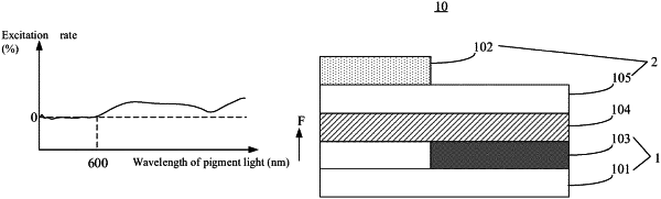
1. An array substrate, comprising a base substrate and an organic light-emitting diode (OLED), a photoelectric conversion layer and a light-filtering layer which are on the base substrate; wherein
the photoelectric conversion layer, the light-filtering layer and the OLED are all on a same side of the base substrate, the photoelectric conversion layer and the light-filtering layer are arranged in sequence along a direction away from the base substrate; and
a maximum wavelength of light through the light-filtering layer is not greater than 600 nanometers.
|