| CPC H10K 59/1315 (2023.02) [H10K 50/844 (2023.02); H10K 59/122 (2023.02); H10K 59/124 (2023.02); H10K 77/111 (2023.02); H10K 2102/311 (2023.02)] | 18 Claims |
|
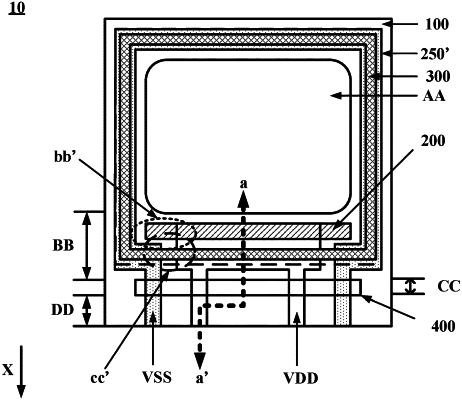
1. A display substrate, comprising:
a substrate comprising a display region and a peripheral region surrounding the display region, the peripheral region comprising a first wiring region, the first wiring region comprising a first sub-wiring region disposed along a first direction away from the display region;
a first conductive layer located on the substrate, the first conductive layer comprising a first portion located in the peripheral region, the first portion of the first conductive layer comprising a first wiring located in the first wiring region;
a first dielectric layer located on the first conductive layer;
a second conductive layer located on the first dielectric layer, the second conductive layer comprising a first portion located in the peripheral region, wherein the first portion of the second conductive layer comprises a second wiring located in the first wiring region, the first wiring and the second wiring being spaced apart from each other along a direction parallel to the substrate;
a second dielectric layer located on the second conductive layer;
a third conductive layer located on the second dielectric layer, the third conductive layer comprising a first portion located in the peripheral region, wherein the first portion of the third conductive layer comprises a third wiring located in the first wiring region;
a third dielectric layer as a planarization layer located on the third conductive layer;
a fourth conductive layer located on the third dielectric layer, the fourth conductive layer comprising a first portion located in the peripheral region, the first portion of the fourth conductive layer comprising a fourth wiring located in the first sub-wiring region,
wherein the fourth wiring is electrically connected to the third wiring,
an orthographic projection of the fourth wiring on the substrate at least partially overlaps with an orthographic projection of the third wiring on the substrate,
the third dielectric layer comprises a first via exposing the third wiring located in the first sub-wiring region,
the fourth wiring is connected to the third wiring via the first via, and
the first via comprises a first array of first sub-vias and a second array of second sub-vias, the first sub-vias and the second sub-vias being configured such that at least one of the first sub-vias is surrounded by the second sub-vias closest to the at least one first sub-via, and at least one of the second sub-vias is surrounded by the first sub-vias closest to the at least one second sub-via.
|