| CPC H10K 59/131 (2023.02) [G09G 3/3688 (2013.01); H10K 59/1213 (2023.02); H10K 59/1216 (2023.02); H10K 59/123 (2023.02); H10K 59/124 (2023.02); G09G 2300/0842 (2013.01); G09G 2310/0262 (2013.01); H01L 27/1214 (2013.01)] | 19 Claims |

|
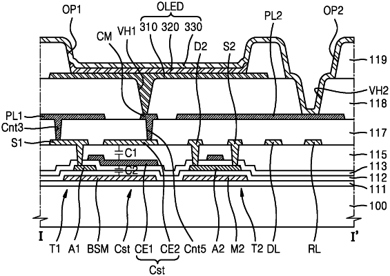
1. A display device, comprising:
a substrate;
a plurality of thin film transistors, each of the plurality of thin film transistors includes a semiconductor layer and a gate electrode;
a first insulating layer covering the gate electrode;
a data line on the first insulating layer;
a second insulating layer covering the data line;
a power line on the second insulating layer;
a third insulating layer covering the power line; and
a pixel electrode on the third insulating layer, wherein
the power line at least partially overlaps at least one of the plurality of thin film transistors,
the power line comprises a first power line and a second power line spaced apart from the first power line,
the first power line is disposed on a same layer as the second power line, and
the first power line and the second power line extend in a same direction as the data line in a plan view.
|