| CPC H10K 59/13 (2023.02) [H10K 59/1213 (2023.02); H10K 59/124 (2023.02); H10K 59/126 (2023.02); H10K 59/131 (2023.02); H10K 59/38 (2023.02); H10K 59/1201 (2023.02)] | 16 Claims |

|
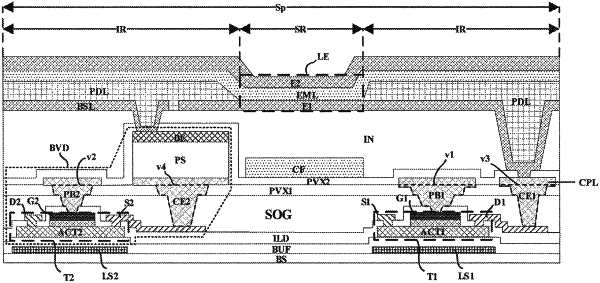
1. A display substrate, comprising a plurality of subpixels;
wherein a respective one of the plurality of subpixels comprises:
a light emitting element;
a first thin film transistor configured to drive light emission of the light emitting element; and
a light emitting brightness value detector;
wherein the light emitting brightness value detector comprises:
a second thin film transistor; and
a photosensor electrically connected to the second thin film transistor and configured to detect a light emitting brightness value;
wherein the display substrate further comprises a stacked structure;
the stacked structure comprises, sequentially,
a base substrate;
the first thin film transistor and the second thin film transistor stacked on the base substrate;
a silicon organic glass layer stacked on at least one of the first thin film transistor or the second thin film transistor;
a conductive protection layer stacked on the silicon organic glass layer; and
the photosensor stacked on the conductive protection layer;
wherein the conductive protection layer extends through the silicon organic glass layer;
the conductive protection layer comprises a first conductive protection block and a second conductive protection block:
an orthographic projection of the first conductive protection block on the base substrate covers the orthographic projection of at least a channel part of the first thin film transistor on the base substrate; and
an orthographic projection of the second conductive protection block on the base substrate covers the orthographic projection of at least a channel part of the second thin film transistor on the base substrate.
|