| CPC H10K 59/122 (2023.02) [H10K 50/15 (2023.02); H10K 50/858 (2023.02); H10K 59/121 (2023.02)] | 14 Claims |

|
1. An organic light-emitting display apparatus comprising:
a substrate;
a plurality of thin film transistors disposed over the substrate;
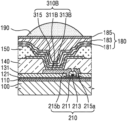
a planarization layer covering the plurality of thin film transistors and having a plurality of via holes for exposing a source electrode or a drain electrode of each of the plurality of thin film transistors;
a plurality of pixel electrodes spaced apart from each other, each of the plurality of pixel electrodes including a first part and a second part, the first part contacting a corresponding one of the plurality of thin film transistors within a corresponding one of the plurality of via holes, the second part disposed on the planarization layer;
a pixel defining layer disposed on the planarization layer and including a plurality of pixel defining holes exposing the plurality of pixel electrodes, wherein each of the plurality of pixel defining holes exposes a center portion and the first and second parts of a corresponding pixel electrode of the plurality of pixel electrodes;
an intermediate layer including a first portion and a second portion, the first portion being disposed on the first part of one pixel electrode of the plurality of pixel electrodes within a corresponding one of the plurality of via holes, the second portion being disposed on the second part of one pixel electrode of the plurality of pixel electrodes; and
a focusing lens disposed over the one pixel electrode and focusing light generated from the intermediate layer and proceeding in a direction away from the pixel electrode.
|