| CPC H10K 59/122 (2023.02) [H04N 23/53 (2023.01); H04N 23/56 (2023.01); H04N 23/63 (2023.01); H10K 50/818 (2023.02); H10K 50/852 (2023.02); H10K 50/858 (2023.02); H10K 59/38 (2023.02); H10K 2102/3026 (2023.02)] | 20 Claims |

|
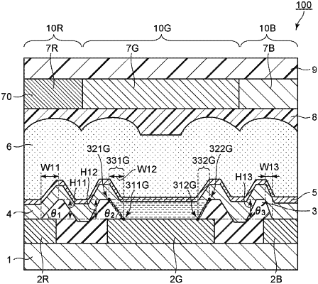
1. An apparatus comprising sub-pixels arranged on a substrate, the sub-pixels including a first sub-pixel, a second sub-pixel, and a third sub-pixel, each of the sub-pixels including a lower electrode, an insulating layer covering an end portion of the lower electrode, an organic layer, and an upper electrode in mentioned order starting from a side closer to the substrate, at least part of the organic layer being continuously arranged in at least two of regions between a position on a first lower electrode included in the first sub-pixel and a position on a second lower electrode included in the second sub-pixel, between the position on the second lower electrode and a position on a third lower electrode included in the third sub-pixel, and between the position on the third lower electrode and the position on the first lower electrode,
wherein the insulating layer has at least one top portion in each of regions between the sub-pixel adjacent to the first sub-pixel and the first sub-pixel, between the sub-pixel adjacent to the second sub-pixel and the second sub-pixel, and between the sub-pixel adjacent to the third sub-pixel and the third sub-pixel, and
wherein formulae (1) and (2) given below are satisfied on an assumption that a portion of the insulating layer between a first end portion of the insulating layer given by an end portion thereof positioned on the first lower electrode and a first top portion given by the top portion closest to the first end portion is called a first portion,
that a portion of the insulating layer between a second end portion of the insulating layer given by an end portion thereof positioned on the second lower electrode and a second top portion given by the top portion closest to the second end portion is called a second portion, and
that a portion of the insulating layer between a third end portion of the insulating layer given by an end portion thereof positioned on the third lower electrode and a third top portion given by the top portion closest to the third end portion is called a third portion:
λ1>λ2>λ3 (1)
θ1<θ2<θ3 (2)
(where, in the formula (1), λ1 denotes a wavelength at which light emitted from the first sub-pixel has maximum intensity, λ2 denotes a wavelength at which light emitted from the second sub-pixel has maximum intensity, and λ3 denotes a wavelength at which light emitted from the third sub-pixel has maximum intensity, and where, in the formula (2), θ1 denotes an inclination angle of the first portion relative to the substrate, θ2 denotes an inclination angle of the second portion relative to the substrate, and θ3 denotes an inclination angle of the third portion relative to the substrate).
|