| CPC H10K 59/1213 (2023.02) [H10K 59/1216 (2023.02); H10K 59/123 (2023.02); H10K 59/124 (2023.02)] | 8 Claims |

|
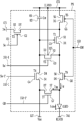
1. An organic light emitting diode display, comprising:
a first thin film transistor disposed on a substrate, the first thin film transistor including a channel formed in a polycrystalline semiconductor layer;
a second thin film transistor disposed on the substrate, the second thin film transistor including a channel formed in an oxide semiconductor layer;
an organic light emitting diode electrically connected to the first thin film transistor;
a storage capacitor having a first electrode and a second electrode, wherein the second electrode of the storage capacitor is electrically connected to a gate electrode of the first thin film transistor; and
an overlapping layer overlapping the oxide semiconductor layer in a plan view and receiving a positive voltage,
wherein the overlapping layer is disposed under the oxide semiconductor layer, and
wherein the oxide semiconductor layer is positioned higher than the gate electrode of the first thin film transistor and the second electrode of the storage capacitor.
|