| CPC H10K 50/8445 (2023.02) [G03F 7/0007 (2013.01); G03F 7/028 (2013.01); G03F 7/095 (2013.01); G03F 7/202 (2013.01); G03F 7/24 (2013.01); G09F 9/301 (2013.01); H10K 71/00 (2023.02); H10K 77/111 (2023.02); H10K 2102/311 (2023.02)] | 8 Claims |

|
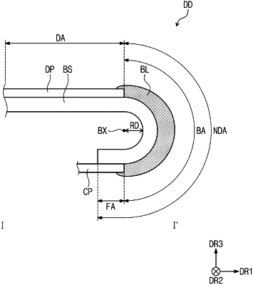
1. A display device comprising:
a flexible substrate comprising:
a display area; and
a non-display area disposed on at least one side of the display area and comprising a bending part;
a display panel disposed on the display area;
a polarization plate disposed on the display panel;
a protection layer disposed on the non-display area and having a modulus value of 500 MPa to 1,200 Mpa; and
a connection circuit member disposed on the non-display area and electrically connected to the display panel,
wherein:
the protection layer does not contact the polarization plate,
the protection layer is disposed between the display panel and the connection circuit member to overlap a portion of at least one of the display panel or the connection circuit member; and
a thickness of a central portion of the protection layer is greater than a thickness of a portion of the protection layer adjacent to, and not overlapping an upper surface of, the display panel and a thickness of a portion of the protection layer adjacent to, and not overlapping a lower surface of, the connection circuit member.
|