| CPC H10K 50/844 (2023.02) [H10K 50/82 (2023.02); H10K 59/123 (2023.02); H10K 59/131 (2023.02); H10K 2102/351 (2023.02)] | 20 Claims |

|
1. A display device comprising:
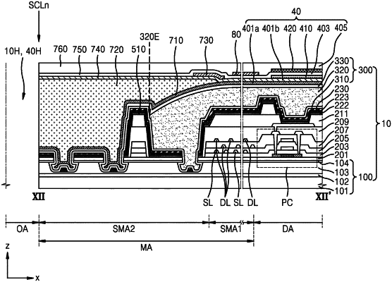
a substrate including a hole and a display area surrounding the hole;
a pixel electrode located in the display area;
an opposite electrode disposed on the pixel electrode, the opposite electrode overlapping the pixel electrode in the display area;
an intermediate layer disposed between the pixel electrode and the opposite electrode in the display area;
an encapsulation layer disposed on the opposite electrode, the encapsulation layer including at least one inorganic encapsulation layer and at least one organic encapsulation layer;
an input sensing layer disposed on the encapsulation layer, wherein the input sensing layer includes a plurality of touch electrodes in the display area;
a planarization layer disposed on the substrate and located in an intermediate area between the hole and the display area, wherein the planarization layer does not overlap the pixel electrode, and a first edge of the planarization layer is located between the display area and a second edge of the planarization layer; and
a cover layer at least partially covering the first edge of the planarization layer and exposing the second edge of the planarization layer, wherein the cover layer and at least one of the touch electrodes are disposed on a same layer.
|