| CPC H10K 50/824 (2023.02) [H10K 59/1216 (2023.02); H10K 59/122 (2023.02); H10K 59/124 (2023.02); H10K 59/126 (2023.02); H10K 59/1315 (2023.02); H10K 71/00 (2023.02); H10K 59/1201 (2023.02)] | 12 Claims |

|
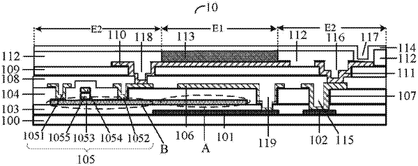
1. An array substrate, comprising:
a base;
light shield layers and a first auxiliary electrode that are disposed on the base;
at least one insulating layer covering the light shield layers and the first auxiliary electrode;
first electrodes that are disposed on the at least one insulating layer;
a conductive connection portion electrically connected to the first auxiliary electrode through a via that penetrates through the at least one insulating layer;
a pixel definition layer defining light-emitting regions and covering the conductive connection portion;
organic light-emitting layers disposed on the first electrodes and located in the light-emitting regions defined by the pixel definition layer; and
at least one second electrode covering the pixel definition layer and the organic light-emitting layers, and a second electrode in the at least one second electrode being electrically connected to the conductive connection portion through a via that penetrates through the pixel definition layer;
wherein the at least one insulating layer includes:
a buffer layer covering the light shield layers and the first auxiliary electrode, and an interlayer dielectric layer disposed on the buffer layer; the via that penetrates through the at least one insulating layer including a first via that penetrates through the interlayer dielectric layer and the buffer layer; and
the conductive connection portion includes:
a second auxiliary electrode disposed on the interlayer dielectric layer, the second auxiliary electrode being electrically connected to the first auxiliary electrode through the first via that penetrates through the interlayer dielectric layer and the buffer layer;
wherein the at least one insulating layer further includes:
a planarization layer covering the second auxiliary electrode;
the via that penetrates through the at least one insulating layer including a second via that penetrates through the planarization layer; and
the conductive connection portion further includes:
a third auxiliary electrode disposed on the planarization layer, the third auxiliary electrode and the first electrode being disposed in a same layer;
the third auxiliary electrode is electrically connected to the second auxiliary electrode through the second via that penetrates through the planarization layer; and
the via that penetrates through the pixel definition layer is a third via, and the second electrode is electrically connected to the third auxiliary electrode through the third via;
the array substrate further comprising:
thin film transistors disposed between the buffer layer and the planarization layer, a first electrode in the first electrodes being electrically connected to a corresponding thin film transistor through a fourth via that penetrates through the planarization layer;
wherein active layers of the thin film transistors are disposed between the buffer layer and the interlayer dielectric layer, and sources and drains of the thin film transistors are disposed on the interlayer dielectric layer;
an active layer in the active layers includes a first portion that overlaps with a corresponding organic light-emitting layer in a direction perpendicular to the base and a second portion that is non-overlapping with the corresponding organic light-emitting layer in the direction perpendicular to the base, and a source and a drain of a thin film transistor in the thin film transistors are electrically connected to a second portion of a corresponding active layer through vias that penetrate through the interlayer dielectric layer, respectively; and
capacitor electrodes disposed between the interlayer dielectric layer and the planarization layer, a capacitor electrode in the capacitor electrodes being directly electrically connected to a corresponding light shield layer through a fifth via that penetrates through the interlayer dielectric layer and the buffer layer, and partially overlapping with the corresponding active layer.
|