| CPC H10K 30/80 (2023.02) [H10K 39/32 (2023.02); G06V 40/1318 (2022.01)] | 19 Claims |

|
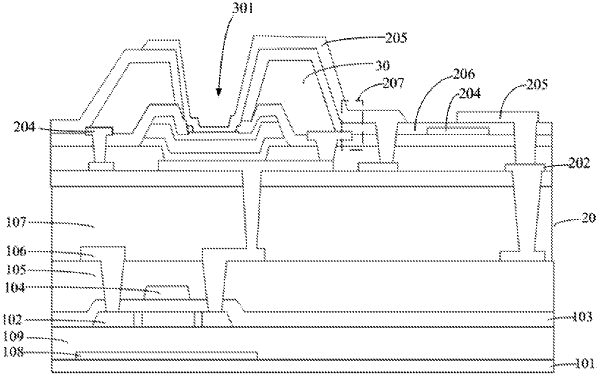
1. An array substrate, comprising:
a base substrate;
a light-sensitive component layer disposed on the base substrate, wherein a plurality of light-sensitive components are disposed at intervals on the light-sensitive component layer;
a first light-shielding layer disposed on the light-sensitive component layer and comprising a plurality of black matrices disposed at intervals, wherein an orthographic projection of the first light-shielding layer on the base substrate partially overlaps with an orthographic projection of each of the light-sensitive components on the base substrate;
a first metal layer disposed on the base substrate, wherein the light-sensitive component comprises a cathode, the first metal layer comprises a touch wire, and the touch wire and the cathode are disposed at intervals in the first metal layer;
a first electrode layer disposed on the light-sensitive components, wherein the first electrode layer comprises a touch electrode, and the touch wire is connected to the touch electrode; and
a second electrode layer disposed on the black matrices, wherein the light-sensitive component comprises an anode, the second electrode layer comprises a pixel electrode, and the pixel electrode and the anode are disposed at intervals in the second electrode layer.
|