| CPC H10B 63/34 (2023.02) [H01L 29/66969 (2013.01); H01L 29/78642 (2013.01); H01L 29/7869 (2013.01); H10B 53/30 (2023.02); H10B 53/40 (2023.02); H10B 63/80 (2023.02); H10N 70/011 (2023.02); H10N 70/231 (2023.02); H10N 70/24 (2023.02)] | 20 Claims |
|
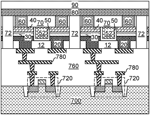
1. A device structure comprising at least one selector device, wherein each of the at least one selector device comprises:
a vertical stack including a bottom electrode, a metal oxide semiconductor channel layer, and a top electrode and located over a substrate;
a gate dielectric layer contacting a sidewall of the bottom electrode;
a gate electrode laterally surrounded by the gate dielectric layer;
a via-level dielectric layer underlying the gate dielectric layer and laterally surrounding a via portion of the bottom electrode; and
dielectric isolation structure contacting an additional sidewall of the bottom electrode and contacting a sidewall of the top electrode.
|