| CPC H10B 63/00 (2023.02) [G11C 5/025 (2013.01); G11C 13/0002 (2013.01); G11C 13/0004 (2013.01); H10N 70/231 (2023.02); H10N 70/826 (2023.02); H10N 70/8828 (2023.02)] | 12 Claims |

|
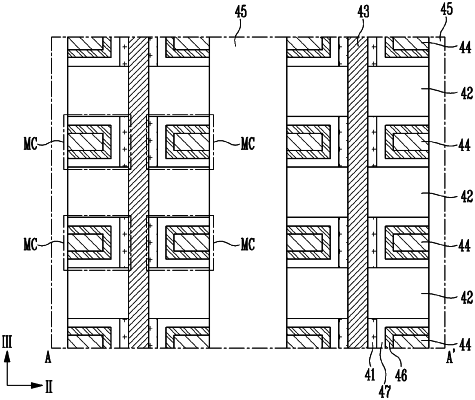
1. A semiconductor memory comprising:
first variable resistance layers and insulating layers alternately stacked;
conductive pillars passing through the first variable resistance layers and the insulating layers;
a slit insulating layer vertically passing through the insulating layers, extending in a first direction, and being disposed in a second direction of the insulating layers, the second direction intersecting with the first direction;
conductive layers disposed between the slit insulating layer and the first variable resistance layers; and
electrode layers disposed between the conductive layers and the first variable resistance layers, each of the electrode layers being in contact with the slit insulating layer,
wherein the first variable resistance layers remain in an amorphous state during a program operation.
|