US 12,075,631 B2
Magnetic random access memory and manufacturing method thereof
Ji-Feng Ying, Hsinchu (TW); and Duen-Huei Hou, Hsinchu (TW)
Assigned to TAIWAN SEMICONDUCTOR MANUFACTURING COMPANY, LTD., Hsinchu (TW)
Filed by TAIWAN SEMICONDUCTOR MANUFACTURING COMPANY, LTD., Hsinchu (TW)
Filed on Apr. 24, 2023, as Appl. No. 18/138,625.
Application 18/138,625 is a continuation of application No. 17/316,406, filed on May 10, 2021, granted, now 11,659,718.
Application 17/316,406 is a continuation of application No. 16/743,992, filed on Jan. 15, 2020, granted, now 11,004,901, issued on May 11, 2021.
Application 16/743,992 is a continuation of application No. 16/019,394, filed on Jun. 26, 2018, granted, now 10,541,269, issued on Jan. 21, 2020.
Prior Publication US 2023/0269951 A1, Aug. 24, 2023
This patent is subject to a terminal disclaimer.
Int. Cl. H10B 61/00 (2023.01); B82Y 25/00 (2011.01); G11C 11/16 (2006.01); H10N 50/01 (2023.01); H10N 50/10 (2023.01); H10N 50/80 (2023.01); H10N 50/85 (2023.01)
CPC H10B 61/22 (2023.02) [G11C 11/161 (2013.01); H10N 50/01 (2023.02); H10N 50/10 (2023.02); H10N 50/80 (2023.02); H10N 50/85 (2023.02); B82Y 25/00 (2013.01)] 20 Claims
OG exemplary drawing
 
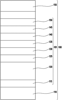
1. A magnetic random access memory (MRAM), comprising:
a first magnetic layer disposed over a substrate;
a first non-magnetic layer disposed over the first magnetic layer;
a second magnetic layer disposed over the first non-magnetic layer;
a second non-magnetic layer disposed over the second magnetic layer; and
a third non-magnetic layer disposed over the second non-magnetic layer, wherein:
the second magnetic layer includes a plurality of magnetic material pieces,
the plurality of magnetic material pieces are in direct contact with the first non-magnetic layer, and
when viewed from above, shapes of the plurality of magnetic material pieces includes a circular shape, an oval shape or a cloud-shape.