| CPC H10B 53/30 (2023.02) [H01L 28/60 (2013.01)] | 20 Claims |
|
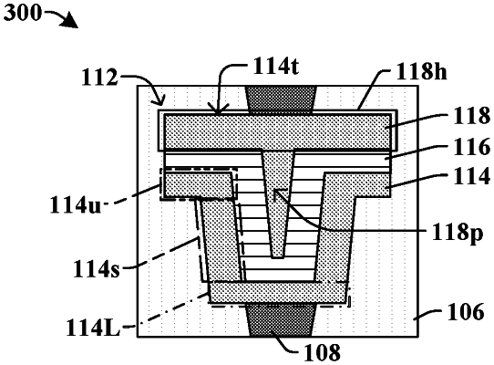
1. An integrated chip, comprising:
a first interconnect dielectric layers over a substrate and surrounding a first wire;
a second interconnect dielectric layer over the first interconnect dielectric layer and surrounding a first via;
a bottom electrode disposed over a conductive structure and extending through the first interconnect dielectric layer and the second interconnect dielectric layer;
a top electrode disposed over the bottom electrode; and
a ferroelectric layer disposed between and contacting the bottom electrode and the top electrode, wherein the ferroelectric layer comprises a first lower horizontal portion, a first upper horizontal portion arranged above the first lower horizontal portion, and a first sidewall portion coupling the first lower horizontal portion to the first upper horizontal portion, wherein the first lower horizontal portion is below an entirety of the second interconnect dielectric layer, and wherein the first upper horizontal portion is above the entirety of the second interconnect dielectric layer.
|