| CPC H10B 43/35 (2023.02) [H10B 41/10 (2023.02); H10B 41/27 (2023.02); H10B 41/35 (2023.02); H10B 41/40 (2023.02); H10B 43/10 (2023.02); H10B 43/27 (2023.02); H10B 43/40 (2023.02)] | 11 Claims |

|
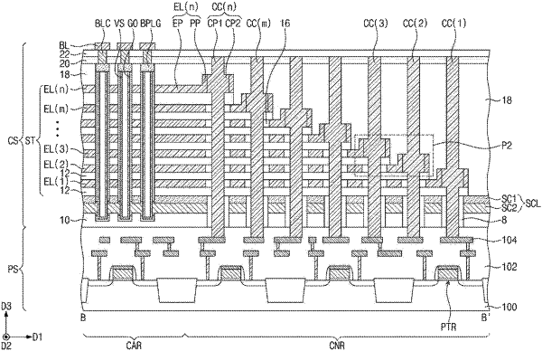
1. A three-dimensional semiconductor memory device, comprising:
a first substrate that comprises a cell array region and a connection region;
a first electrode layer and a second electrode layer that are sequentially stacked and spaced apart from each other on the first substrate, and an end portion of the first electrode layer and an end portion of the second electrode layer are offset from each other on the connection region;
a first cell contact penetrating the second electrode layer and the first electrode layer such as to be connected to the second electrode layer on the connection region; and
a first contact dielectric pattern between the first cell contact and the first electrode layer,
wherein the first cell contact comprises:
a columnar part that vertically extends from a top surface of the first substrate; and
a connection part that laterally protrudes from the columnar part and contacts the second electrode layer,
wherein a width of the connection part is less than a width of the first contact dielectric pattern, and
wherein the second electrode layer is stacked on a top surface of the first electrode layer, and an uppermost surface of the first contact dielectric pattern is below the second electrode layer.
|