| CPC H10B 43/27 (2023.02) [H01L 23/481 (2013.01); H10B 41/10 (2023.02); H10B 41/27 (2023.02); H10B 41/35 (2023.02); H10B 41/40 (2023.02); H10B 43/10 (2023.02); H10B 43/35 (2023.02); H10B 43/40 (2023.02)] | 20 Claims |

|
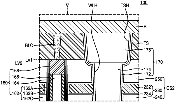
1. An integrated circuit device comprising:
a substrate;
a lower base layer and an upper base layer sequentially stacked on the substrate;
a first gate stack extending on the upper base layer in a first direction that is parallel to a main surface of the substrate, the first gate stack including a plurality of first gate electrodes and a plurality of first insulating layers alternately stacked in a second direction that is perpendicular to the main surface of the substrate;
a second gate stack extending on the first gate stack in the first direction and including a plurality of second gate electrodes and a plurality of second insulating layers alternately stacked in the second direction;
a channel structure extending through the first gate stack and the second gate stack in the second direction;
a word line cut opening extending through the first gate stack and the second gate stack in the second direction and extending in the first direction;
an upper support layer on the second gate stack and comprising a plurality of holes, each of which overlaps the word line cut opening in the second direction and comprises a portion that overlaps the second gate stack in the second direction and in a third direction that is parallel to the main surface of the substrate and is perpendicular to the first direction; and
an insulating structure in the word line cut opening and the plurality of holes,
wherein an upper surface of the channel structure is in contact with a lower surface of the upper support layer,
wherein an upper surface of an uppermost one of the plurality of second insulating layers is higher than respective lowermost ends of the plurality of holes, and
wherein the upper surface of the channel structure is higher than the respective lowermost ends of the plurality of holes.
|