| CPC H10B 43/27 (2023.02) [G11C 7/18 (2013.01); G11C 8/14 (2013.01); H01L 23/528 (2013.01); H10B 41/10 (2023.02); H10B 41/27 (2023.02); H10B 41/40 (2023.02); H10B 43/10 (2023.02); H10B 43/40 (2023.02)] | 25 Claims |

|
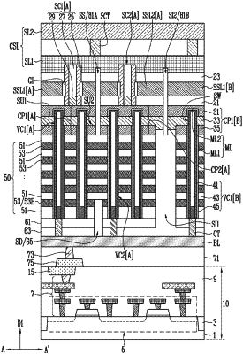
1. A semiconductor memory device comprising:
a bit line overlapping with a peripheral circuit layer;
a source layer over the bit line;
interlayer insulating layers and conductive patterns alternately stacked in a first direction between the bit line and the source layer;
vertical channels connected to the bit line, the vertical channels penetrating the interlayer insulating layers and the conductive patterns, the vertical channels protruding farther in the first direction than the stacked interlayer insulating layers and the conductive patterns;
a connection pattern in contact with a portion of each of the vertical channels that protrudes farther in the first direction than the stacked interlayer insulating layers and the conductive patterns, the connection pattern connecting the vertical channels;
a source channel in contact with the connection pattern, the source channel extending in the first direction to contact the source layer; and
a source select line surrounding the source channel and spaced apart from the connection pattern and the source layer so that the source layer is electrically connected to the connection pattern via the source channel depending on a signal applied to the source select line.
|