US 12,075,613 B2
Buried word line of a dynamic random access memory and method for fabricating the same
Pin-Hong Chen, Tainan (TW); Yi-Wei Chen, Taichung (TW); Tzu-Chieh Chen, Pingtung County (TW); Chih-Chieh Tsai, Kaohsiung (TW); Chia-Chen Wu, Nantou County (TW); Kai-Jiun Chang, Taoyuan (TW); Yi-An Huang, New Taipei (TW); and Tsun-Min Cheng, Changhua County (TW)
Assigned to UNITED MICROELECTRONICS CORP., Hsin-Chu (TW); and Fujian Jinhua Integrated Circuit Co., Ltd., Quanzhou (CN)
Filed by UNITED MICROELECTRONICS CORP., Hsin-Chu (TW); and Fujian Jinhua Integrated Circuit Co., Ltd., Quanzhou (CN)
Filed on Jan. 6, 2022, as Appl. No. 17/570,345.
Application 17/570,345 is a division of application No. 15/712,151, filed on Sep. 22, 2017, granted, now 11,251,187.
Claims priority of application No. 201710733801.2 (CN), filed on Aug. 24, 2017.
Prior Publication US 2022/0130839 A1, Apr. 28, 2022
Int. Cl. H10B 12/00 (2023.01)
CPC H10B 12/488 (2023.02) [H10B 12/34 (2023.02)] 11 Claims
OG exemplary drawing
 
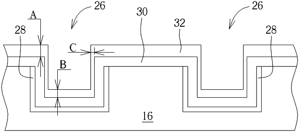
1. A method for fabricating buried word line of a dynamic random access memory (DRAM), comprising:
forming a trench in a substrate, wherein the substrate is a single-layer semiconductor substrate made of a single material;
forming a first conductive layer in the trench;
forming a second conductive layer on the first conductive layer, wherein the second conductive layer above the substrate and the second conductive layer below the substrate comprise different thickness; and
forming a third conductive layer on the second conductive layer to fill the trench.