| CPC H10B 12/0335 (2023.02) [H10B 12/053 (2023.02); H10B 12/09 (2023.02); H10B 12/315 (2023.02); H10B 12/34 (2023.02); H10B 12/482 (2023.02); H10B 12/485 (2023.02); H10B 12/50 (2023.02)] | 6 Claims |
|
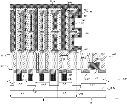
1. A semiconductor device, comprising:
multiple core components comprising active areas; and
multiple contact plugs in the semiconductor device, wherein the contact plugs comprises first contact plugs and at least one second contact plug, and the at least one second contact plug is in a shape of inverted-U or comb, and a bottom of each of the contact plugs contacts the active area;
a plurality of first capacitors directly contact on the first contact plugs; and
a second capacitor directly contact on the at least one second contact plug;
wherein a topmost surface of the at least one second contact plug is not lower than a topmost surface of the first contact plug.
|