| CPC H04R 31/00 (2013.01) [H04R 19/04 (2013.01); H04R 2201/003 (2013.01); H04R 2410/03 (2013.01)] | 14 Claims |

|
1. A process of fabricating a capacitive microphone comprising:
(A) fabricating a first capacitor and a second capacitor, and configuring the two capacitors so that a signal output S1 of the first capacitor is substantially (±5%) the additive inverse of a signal output S2 of the second capacitor, and a total signal output St is a difference between S1 and S2; and
wherein fabricating the first capacitor comprises fabricating a first electrical conductor ECA1, fabricating a second electrical conductor ECA2, and configuring conductors ECA1 and ECA2 in a lateral mode as defined in the following:
wherein conductors ECA1 and ECA2 have a mutual capacitance therebetween;
wherein said mutual capacitance can be varied by an acoustic pressure impacting upon ECA1 and/or ECA2 along a range of impacting directions in 3D space, generating the signal output S1 of the first capacitor;
wherein said mutual capacitance is varied the most by an acoustic pressure impacting upon ECA1 and/or ECA2 along one direction among said range of impacting directions, said one direction being defined as the primary direction;
wherein ECA1 has a first projection along said primary direction on a conceptual plane that is perpendicular to said primary direction; and ECA2 has a second projection along said primary direction on the conceptual plane;
wherein the first projection and the second projection have a shortest distance Dmin therebetween, and Dmin remains greater than zero regardless of that ECA1 and/or ECA2 is (are) impacted by an acoustic pressure along said primary direction or not;
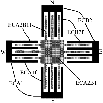
wherein fabricating the second capacitor comprises fabricating a third electrical conductor ECB1 and a fourth electrical conductor ECB2, and configuring the conductors ECB1 and ECB2 in a lateral mode too;
wherein the process further comprises configuring the two capacitors so that the first capacitor and the second capacitor share a same primary direction;
wherein the process further comprises a step (Pre-A) before step (A), providing a substrate, wherein the substrate can be viewed as said conceptual plane; and constructing conductors ECA1 and ECA2 above the substrate side-by-side and constructing conductors ECB1 and ECB2 above the substrate side-by-side too;
wherein the process further comprises configuring one of conductors ECA1 and ECA2 so that it is electrically connected to one of conductors ECB1 and ECB2 to form a single shared conductor;
wherein the process further comprises configuring both conductors ECA1 and ECB2 so that they are fixed relative to the substrate, and fabricating single conductor ECA2B1 so that it comprises a membrane that is movable relative to the substrate, and said primary direction is perpendicular to the membrane plane; and
wherein the process further comprises:
fabricating conductor ECA1 so that it comprises a flat layer in parallel to the substrate and having a thickness ECA1t and a height ECA1h along the primary direction as measured from the substrate;
fabricating conductor ECB2 so that it comprises a flat layer in parallel to the substrate and having a thickness ECB2t and a height ECB2h along the primary direction as measured from the same substrate;
fabricating single conductor ECA2B1 so that it comprises a portion ECA2* facing conductor ECA1, wherein portion ECA2* comprises a flat layer parallel to the substrate and having a thickness ECA2*t and a height ECA2*h along the primary direction as measured from the same substrate; and
fabricating single conductor ECA2B1 so that it comprises a portion ECB1* facing conductor ECB2, wherein portion ECB1* comprises a flat layer in parallel to the substrate and having a thickness ECB1*t and a height ECB1*h along the primary direction as measured from the same substrate.
|