| CPC H04N 25/778 (2023.01) [H01L 27/14612 (2013.01); H04N 25/53 (2023.01); H04N 25/709 (2023.01); H04N 25/75 (2023.01); H04N 25/79 (2023.01)] | 19 Claims |

|
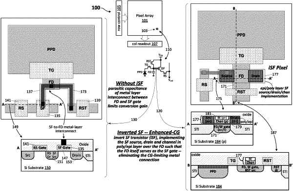
1. An integrated-circuit pixel comprising:
a silicon substrate having a photodetection element and a floating diffusion node formed therein;
an oxide region; and
a semiconductor region disposed on the oxide region opposite the silicon substrate and having (i) conductively doped regions at either end to form source and drain terminals of a field-effect transistor and (ii) a channel region between the source and drain terminals and situated opposite the oxide layer from the floating diffusion node such that the floating diffusion node implements a gate of the field-effect transistor,
wherein the semiconductor region has a first carrier concentration and wherein a bulk-emulation sub-region of the semiconductor region has a second carrier concentration higher than the first p-type carrier concentration.
|