| CPC H04N 25/683 (2023.01) | 20 Claims |

|
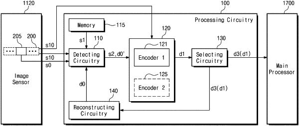
1. An image processing block comprising:
an image sensor including a plurality of pixels configured to receive a light from outside, the image sensor configured to generate pixel values of the plurality of pixels based on the received light; and
a processor configured to:
identify an abnormal pixel among the plurality of pixels based on the pixel values;
generate at least one of a first encoded data or a second encoded data by encoding pixel data of the plurality of pixels based on remaining pixels of the plurality of pixels excluding the identified abnormal pixel; and
output a third encoded data based on the at least one first encoded data or the second encoded data.
|