| CPC H03K 3/017 (2013.01) [G06F 1/08 (2013.01); G06F 1/12 (2013.01)] | 16 Claims |

|
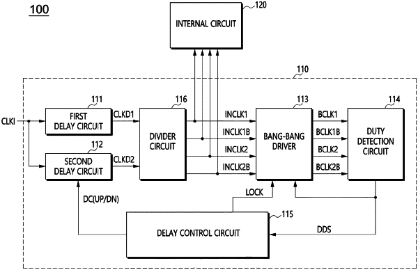
1. A duty correction circuit comprising:
a first delay circuit configured to delay an input clock signal to generate a first delayed clock signal;
a second delay circuit configured to variably delay the input clock signal based on a delay control signal to generate a second delayed clock signal;
a bang-bang driver configured to:
drive the first and second delayed clock signals to generate a first driving clock signal and a second driving clock signal; and
delay the first and second driving clock signals based on a locking signal and a duty detection signal;
a duty detection circuit configured to detect duty cycles of the first and second driving clock signals and generate the duty detection signal; and
a delay control circuit configured to generate the locking signal and the delay control signal based on the duty detection signal.
|