| CPC H03K 19/007 (2013.01) [H03K 19/00384 (2013.01)] | 20 Claims |

|
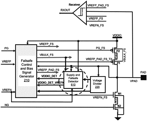
1. A circuit of a chip, comprising:
an I/O circuit comprising a transistor connected to an I/O pad, wherein the I/O pad is connected to one or more other chips via an I/O bus;
a supply and failsafe detector component comprising:
a first input connected to an I/O supply voltage of the chip,
a second input connected to the I/O pad and receiving an I/O pad voltage as supply,
an I/O supply output signal generated by the supply and failsafe detector component, the I/O supply output signal having a low voltage value when the I/O supply voltage of the chip is below a medium voltage level and the I/O supply output signal having a high voltage value when the I/O supply voltage of the chip is above the medium voltage level, wherein the medium voltage level is above a threshold voltage of the transistor of the I/O circuit and below the high voltage value; and
a multiplexer controlled by the I/O supply output signal, the multiplexer providing a reference voltage as input to the transistor of the I/O circuit.
|