| CPC H03G 3/3042 (2013.01) [H03F 1/0211 (2013.01); H03F 1/302 (2013.01); H03F 3/245 (2013.01); H04B 1/04 (2013.01); H01L 23/66 (2013.01); H01L 2223/6644 (2013.01); H03F 1/56 (2013.01); H03F 2200/222 (2013.01); H03F 2200/451 (2013.01); H03G 2201/708 (2013.01)] | 12 Claims |

|
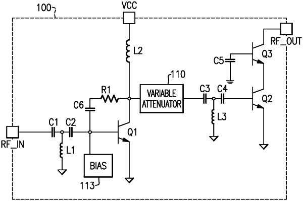
1. A power amplifier comprising:
an input stage that includes an amplifying transistor having an input node and an output node, such that a signal at the input node has a first power level and an amplified signal at the output node has a second power level;
a bias circuit configured to provide a bias signal to the amplifying transistor;
a feedback circuit that couples the output node of the amplifying transistor to the input node of the amplifying transistor, the feedback circuit including a resistance and a capacitance arranged in series; and
a gain compensation circuit implemented along an output path from the output node of the amplifying transistor, such that the gain compensation circuit adjusts the second power level based on a variation in temperature associated with the power amplifier.
|