| CPC H03F 1/0227 (2013.01) [H02M 1/0025 (2021.05); H02M 3/158 (2013.01); H03F 3/245 (2013.01); H03F 3/72 (2013.01); H03F 2203/7227 (2013.01)] | 20 Claims |

|
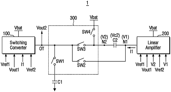
9. A semiconductor device comprising:
an output terminal;
a switching converter configured to control an output voltage output from the output terminal based on a first reference voltage and a power supply voltage;
a load capacitor configured to be charged with a voltage corresponding to the output voltage;
a linear amplifier connected to one end of an alternating current (AC) coupling capacitor and configured to control a voltage of the AC coupling capacitor based on a second reference voltage and the power supply voltage;
a first switch configured to control a connection between the output terminal and the load capacitor;
a second switch configured to control a connection between the output terminal and the one end of the AC coupling capacitor; and
a third switch configured to control a connection between the output terminal and another end of the AC coupling capacitor.
|