|
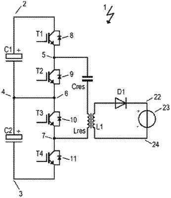
1. A circuit arrangement for balancing a split DC link, which comprises a series circuit comprising a first DC-link capacitor and a second DC-link capacitor between a first DC-voltage terminal and a second DC-voltage terminal and the series circuit comprising a DC-link center point between the first DC-link capacitor and the second DC-link capacitor, wherein the first DC-voltage terminal is further connected via a first semiconductor switch to a first intermediate point, the first intermediate point is connected via a second semiconductor switch to a bridge center point, the bridge center point is connected via a third semiconductor switch to a second intermediate point, and the second intermediate point is connected via a fourth semiconductor switch to the second DC-voltage terminal, wherein the first, second, third and fourth semiconductor switches together form a series circuit and each have an antiparallel diode connected thereto, and the circuit arrangement further comprises a resonant circuit comprising a resonant capacitor and a resonant inductor, wherein a first terminal of the resonant capacitor is connected to the first intermediate point, and a second terminal of the resonant capacitor is connected to the DC-link center point via a connecting path, in which the resonant inductor is arranged in a series circuit with the third semiconductor switch, and which runs via the second intermediate point, the circuit arrangement further comprising an additional winding magnetically coupled to the resonant inductor, wherein a first terminal of the additional winding is connected via a first diode to a first terminal of a countervoltage source, and a second terminal of the additional winding is connected to a second terminal of the countervoltage source, wherein an energy coupled into the additional winding from the resonant inductor is discharged into the countervoltage source via the first diode.
|
