| CPC H02M 3/003 (2021.05) [H01L 25/115 (2013.01); H02M 3/33523 (2013.01); H05K 1/181 (2013.01)] | 11 Claims |
|
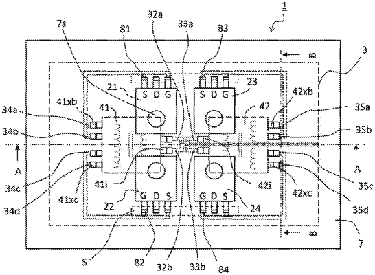
1. A power conversion device, comprising:
semiconductor switching elements each forming a plate shape, which are paired to form a bridge for power conversion;
a housing having a fixing surface to which one of major surfaces of each of the semiconductor switching elements is fixed;
a circuit board on which a driving circuit for driving the semiconductor switching elements is mounted and which is located opposite to and spaced apart from the fixing surface; and
insertion guides which are disposed on an opposing surface of the circuit board relative to the fixing surface;
wherein respective lead terminals of the semiconductor switching elements that are projecting from one lateral sides thereof, each have a length that is matched with a height of a pulse transformer that serves to form the driving circuit, and extend toward the insertion guides; and
wherein the pulse transformer is disposed on the opposing surface so as to be opposite to the other one of the major surfaces of each of the semiconductor switching elements.
|