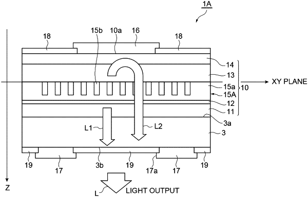
| CPC H01S 5/11 (2021.01) [H01S 5/0216 (2013.01); H01S 5/3211 (2013.01)] | 19 Claims |

|
1. A light-emitting element comprising:
a substrate having a main surface and a rear surface opposing the main surface; and
a semiconductor laminate body provided on the main surface of the substrate and having a lower surface facing the main surface and an upper surface located on an opposite end side of the substrate with respect to the lower surface, the semiconductor laminate body including a first cladding layer provided between the lower surface and the upper surface, a second cladding layer provided between the first cladding layer and the upper surface, an active layer provided between the first cladding layer and the second cladding layer, and a resonance-mode forming layer provided between the first cladding layer and the second cladding layer,
wherein the resonance-mode forming layer includes a basic layer and a plurality of modified refractive index regions configured to each have a refractive index different from that of the basic layer and be distributed in a two-dimensional manner on a set plane perpendicular to a stacking direction of the semiconductor laminate body,
a structure body constituted by the substrate and the semiconductor laminate body has a first structural surface corresponding to the rear surface of the substrate and a second structural surface corresponding to the upper surface of the semiconductor laminate body,
while a region for outputting laser light is provided on one of the first structural surface and the second structural surface of the structure body, on the other surface of the first structural surface and the second structural surface, a metal electrode film having a first layer surface facing the structure body and a second layer surface located on an opposite side to the structure body with respect to the first layer surface is provided,
the metal electrode film includes a first layer configured to have the first layer surface and be in close contact with the structure body via the first layer surface so as to form ohmic contact with the structure body,
a second layer configured to be provided between the first layer and the second layer surface, have a composition different from that of the first layer, and reflect light from the resonance-mode forming layer,
a third layer configured to be provided between the second layer and the second layer surface, have a composition different from that of the second layer, and have a lower diffusion degree than the second layer with respect to a diffusion degree of a solder material, and
a fourth layer for solder bonding configured to be provided between the third layer and the second layer surface, have a composition different from that of the third layer, and have a higher diffusion degree than the third layer with respect to the diffusion degree of the solder material.
|