| CPC H01Q 1/2291 (2013.01) [H01Q 7/00 (2013.01); H01Q 9/0407 (2013.01); H01Q 21/08 (2013.01); H01Q 25/002 (2013.01)] | 17 Claims |

|
1. An electronic device comprising:
a housing;
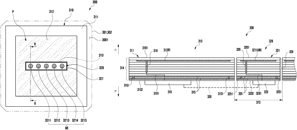
a first antenna structure provided in an inner space of the housing, the first antenna structure comprising:
a first substrate having a first substrate surface facing a first direction and a second substrate surface facing a second direction opposite to the first direction, the first substrate comprising a plurality of first insulating layers and a first ground layer disposed on at least one of the plurality of first insulating layers; and
a conductive patch disposed on one of the plurality of first insulating layers and overlapping the first ground layer when the first substrate surface is viewed from above;
a second antenna structure disposed near the first substrate in the inner space of the housing, the second antenna structure comprising:
a second substrate having a third substrate surface facing the first direction and a fourth substrate surface facing the second direction, the second substrate comprising a plurality of second insulating layers that are stacked and a second ground layer; and
at least two antenna elements disposed on a second insulating layer, among the plurality of second insulating layers, that is closer to the third substrate surface than the fourth substrate surface,
wherein the conductive patch at least partly surrounds the second antenna structure.
|