| CPC H01P 3/121 (2013.01) [H01P 5/107 (2013.01); H01Q 9/045 (2013.01); H05K 1/0218 (2013.01); H05K 1/0298 (2013.01); H05K 1/18 (2013.01); H05K 3/243 (2013.01); H05K 3/429 (2013.01); H05K 3/4652 (2013.01); H05K 3/4664 (2013.01); H05K 3/4697 (2013.01); H05K 2201/0367 (2013.01); H05K 2201/0723 (2013.01); H05K 2201/09981 (2013.01); H05K 2201/09985 (2020.08); H05K 2201/10098 (2013.01); H05K 2201/10507 (2013.01); H05K 2203/0723 (2013.01)] | 19 Claims |

|
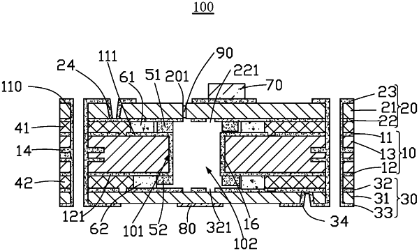
1. An electromagnetic wave transmission board comprising:
an inner board defining a first through hole, wherein a wall of the first through hole is provided with a plated metal layer;
a first outer plate disposed on a side of the inner board and covering one end of the first through hole;
a second outer plate disposed on a side of the inner board away from the first outer plate and covering another end of the first through hole;
a first plated bump disposed between the inner plate and the first outer plate, the first plated bump surrounding the first through hole;
a first conductive bump sandwiched between the inner plate and the first outer plate, the first conductive bump surrounding the first plate bump;
a first adhesive layer sandwiched between the inner plate and the first outer plate and located on a side of the first conductive bump away from the first plated bump;
a second plated bump disposed between the inner plate and the second outer plate, the second plated bump surrounding the first through hole;
a second conductive bump sandwiched between the inner plate and the second outer plate, the second conductive bump surrounding the second plated bump; and
a second adhesive layer sandwiched between the inner plate and the second outer plate and disposed on a side of the second conductive bump away from the second plated bump;
wherein the plated metal layer, the first plated bump, the first conductive bump, the first outer plate, the second plated bump, the second conductive bump, and the second outer plate cooperatively form a chamber, the electromagnetic wave transmission board is configured to transmit electromagnetic wave signal through the chamber.
|